2024-05-13
USB PD on the CH32V003
In a recent post I wrote about USB PD Coding and how to encode and decode the signals in software. In this post I will talk about how to do this on the CH32V003.
Timing
The bitrate of USB PD is 300 kHz, with a tolerance of 10%. For transmission, this implies quite relaxed timing requirements. But for receiving, the constraints are quite tight that way. The sampling (for both input and output) will be done in an assembler routine with busy-wait loops and synchronization with the systick timer.
Tx timing
I'll run the '003 and the systick at 48 MHz. For 600 kHz sampling rate (twice the bitrate), half a bit is 80 clock cycles. This leaves us with enough time to read the data from the ram and write it to the GPIOs. For transmission, I'm not going to use a timer interrupt, but a simple busy-wait loop. It might result in some lost cpu time but will be much easier to implement. The systick will be saved at the beginning and every bit waits for the next systick period of 80 clock cycles.
Rx timing
The receiving part is a bit more complicated. The '003 has a comparator that can be used to detect the signal. The comparator can be set up to trigger an interrupt on a falling edge. The interrupt routine will then start the active wait sampling synchronized by the systick. The systick timer runs at a frequency of 48 MHz. To decode the BMC signal, we need to divide the system clock down to a sampling clock with a fixed rate of at least 3 samples and at most 4 samples per bit (see the previous post). There are two constraints that need to be taken into account for valid clock dividers.
The first one is the bit rate of the signal. The nominal bit rate is 300 kHz, but it has a tolerance of +- 10%. This means that the bit rate can be as low as 270kHz and as high as 330kHz. This is a very wide range and we need to sample the signal with a rate that covers the complete range with at least 3 samples per bit and at most 4 samples per bit. This means that we need to sample the signal with a rate of 3*330 kHz = 990 kHz <= f <= 1080 kHz = 4*270 kHz.
The second constraint is the clock tolerance of the CH32V003. At normal battery charging temperatures, the internal RC oscillator (HSI) has a tolerance of +1.6% and -1.2%. That means with the PLL enabled, the sysclock can be anything between 0.988*48 MHz = 47.424 MHz and 48.768 MHz = 1.016*48 MHz.
I assembled a table of possible clock rates and their nominal, minimum and maximum frequencies.
| div | nom | min | max |
|---|---|---|---|
| 43 | 1.116 | 1.103 | 1.130 |
| 44 | 1.091 | 1.078 | 1.104 |
| 45 | 1.067 | 1.054 | 1.079 |
| 46 | 1.043 | 1.031 | 1.056 |
| 47 | 1.021 | 1.009 | 1.034 |
| 48 | 1.000 | 0.988 | 1.012 |
| 49 | 0.980 | 0.968 | 0.991 |
| 50 | 0.960 | 0.948 | 0.972 |
The dividers 45, 46 and 47 are valid options for the clock divider, because the minimum and the maximum frequency are within the range of our desired sampling clock. Although it would be possible to just use div=46 for some extra safety margin, I decided to use div=47, because it yields one extra clock cycle in the interrupt, freeing more than 2% CPU time for other tasks, compared to div=46.
Signal levels
The nominal voltage level of the USB PD signal is 1.2V, but the CH32V003 only works at a higher logic level. This means that we need some kind of level shifting. I want to be able to use only the '003 and a few passive components, so I decided to use the internal comparator for receiving and a simple voltage divider for the transmission.
Receiving
The comparator is easily set up, its just a voltage reference on one of the inputs and the CC-Signal on the other. Assuming a fixed supply voltage of 3.3V, the reference voltage. The output of the comparator is then used as the receiving GPIO and for decoding. The internal comparator of the '003 is fast enough to catch the signal.
There is no need for hysteresis, since bouncing is only likely to happen at a much higher frequency than the sampling rate. The GPIO interrupt that will be used for the sampling takes some time and will therefore only be able to catch the first edge in a bouncing sequence.
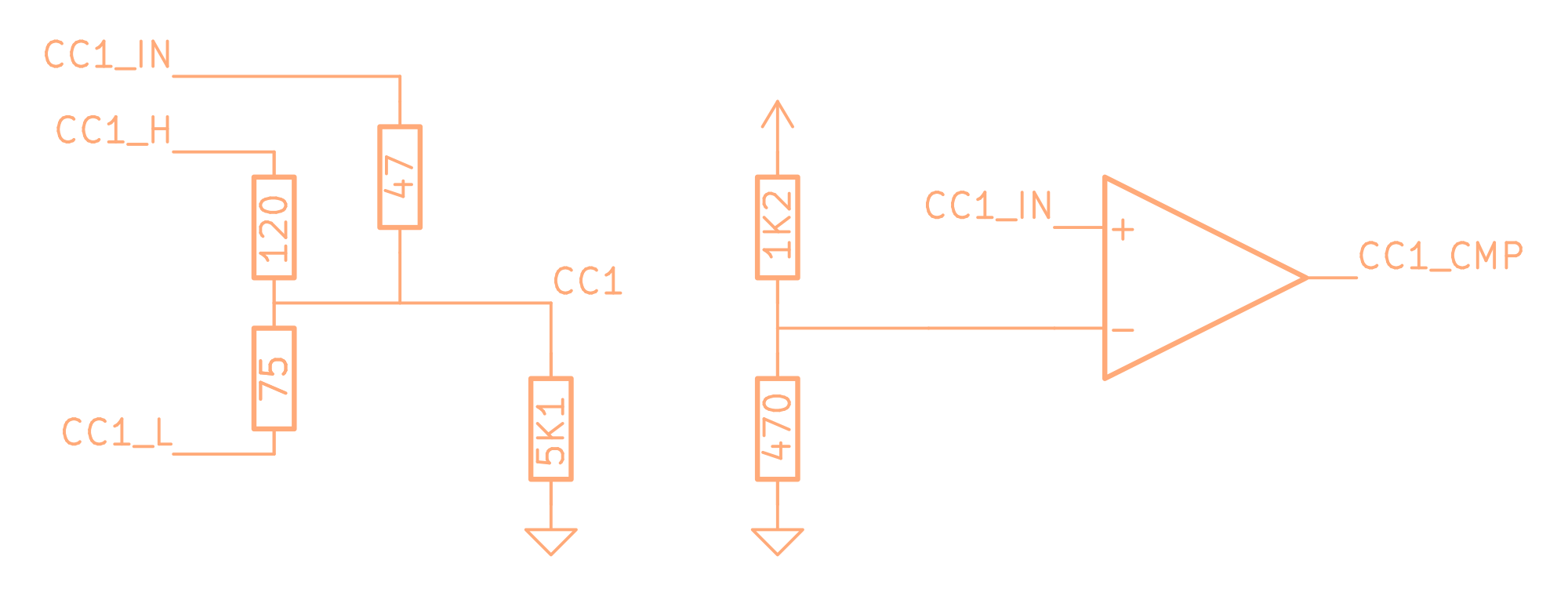
The schematic shows the receiving circuit for one CC line. The CC1_IN signal is the positive input for the comparator, the comparator output is then used as the rx signal.
Transmitting
The transmission stretches the USB-PD specifications quite a bit. Although it would be possible to just use a dedicated push-pull driver, I wanted to use only the '003 passive components. But just using a voltage divider to GND on a single GPIO would put a significant resistive load onto the CC line, even if the '003 is not driving it. At the same time, the resistance of the divider with must be as low as possible to properly drive the line. This combination might cause problems with the other PD device. To avoid this, the low side of the voltage divider is connected to a second GPIO. When the '003 is not driving the CC line, both GPIOs are set to high impedance.
But even that might not be enough to generate a proper signal. The series resistance coming with the voltage divider might be too high to get a proper signal shape. To improve the signal shape (if necessary), one more GPIO is connected to the CC line with a lower resistance as a backup solution. This GPIO can then be used to add a short time "boost" pulses to charge and discharge the CC line faster. The timing of those boost pulses is critical, because the high state might otherwise overshoot the 1.2V level. I don't know yet, whether I'll actually need these boost pulses, but I wanted to have the option for them.
The transceiver schematic shows both the receiving and the transmitting circuit for one CC line. The CC1_H and CC1_L signal are the output GPIOs for the CC1 line. CC1_IN is the input for the comparator and at the same time boost signal for the CC1 line. CC1_IN is fed into the internal comparator of the '003. The comparator output is then used as the rx signal.
Firmware
The timing sensitive part of the firmware is written in assembler, while the rest is written in C. The assembler part is responsible for the sampling of the signal and the en-/decoding of the BMC signal. The C part is responsible to handle the PD protocol and the communication with the other device. So far I implemented
- initialization of GPIOs, comparator and systick
- raw packet transmission and the CRC calculation
- raw packet reception without crc check
- test routines for the transmitter, but not the receiver
It can be found in the ch32v003_usb_pd repository on github: eeucalyptus/ch32v003-usbpd.
Tests
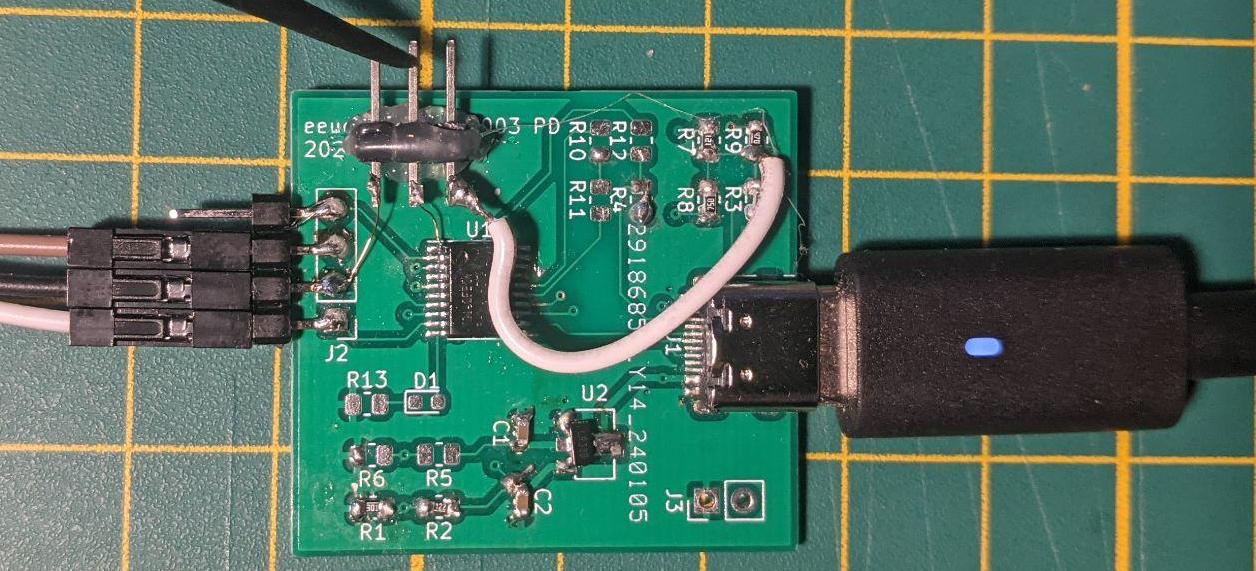
I have tested the transceiver with a simple test setup. The CH32V003 is connected to a WCH-LinkE debug adapter, the comparator output and the high side driver are connected to a logic analyzer. The logic analyzer is set up to decode the BMC signal. The test setup is shown in the picture below.
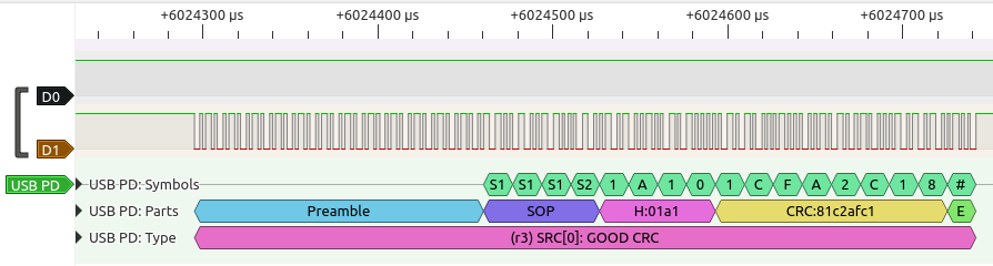
The transmission worked as expected. The output signal shape still has to be tested with a scope and real PD devices, but I was able to decode the transmitted signals with the logic analyzer. The screenshot shows the transmission of a goodcrc message from the '003 to the logic analyzer:
The receiving part of the firmware is not yet tested. Nevertheless, in an older revision of the firmware, I was able to sample the input from a USB PD power supply. The comparator output was sampled with a timer and dma. The signal was printed to the console and manually decoded. This way I was able to verify the input circuit roughly, but the routine was not suitible to decode the signal in real time. I had to rewrite the receiving part completely and this is not yet tested. However, I'm confident that I'll get it running soon.
When just looking at the comparator output with a loopback signal (generated by the output driver), the signal looked a bit funky at first. The rising edges seemed to be quick and crisp, but the falling edges are a bit slow. I thought I had to tune the comparator settings to get a better signal shape. But then I realized that it was a software problem with the output driver: I forgot to set the low side GPIO as an output. The low side GPIO was still high-z and there was therefore no pull-down resistor. This caused the CC line to be significantly overdriven (to 3.3V) and the trigger level of the comparator was still at ~0.9V. After fixing this, the signal looked much better.
Conclusion
So far I was able to send custom messages with the '003 and decode them with a logic analyzer. I was also able to capture a real PD signal with the circuit and decode it offline. There's still a lot of work to do, both on the phy layer (tx, rx) and on the protocol layer. I hope I'll find the time to continue this project soon.
References, Acknowledgements and Misc
Thanks to cnlohr, Cristina, Musicted and the cnlohr_projects discord for the support and the discussions.
My main reference for the USB PD protocol is the USB Power Delivery Specification Revision 3.2 Version 1.0. The specification can be found on here, as well as the USB-C specifications V2.3.
The text and all self produced images are licensed under CC BY-SA 4.0.